PCB Failure Modes, Reliability & Solutions — An XPtronics Inc. Perspective
Pad cratering is a subtle yet serious PCB failure mode where cracking occurs in the laminate beneath a copper pad, separating it from the surrounding resin. Unlike visible defects such as lifted pads or fractured solder joints, pad cratering often remains hidden—leading to intermittent or delayed failures in the field.
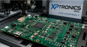
At XPtronics Inc., we frequently see pad cratering emerge in advanced, high-density assemblies where reliability is critical.
Why Pad Cratering Occurs
Pad cratering is driven by a combination of mechanical stress and thermal loading, including:
- PCB flexing during assembly, depanelization, or handling
- Lead-free reflow temperatures that increase thermal stress
- Shock and vibration in industrial, automotive, and embedded systems
- Thinner PCB stackups paired with large or high-I/O components
As electronics continue to get smaller and more complex, the margin for error at the pad-to-laminate interface is reduced.
Reliability Risks in the Field
From a manufacturing and reliability standpoint, pad cratering is especially problematic because it can be:
- Intermittent, failing only under heat or vibration
- Latent, passing functional testing but failing after deployment
- Hard to detect, often requiring X-ray or cross-sectional analysis
Typical failure symptoms include sporadic signal loss, unexpected resets, or intermittent open circuits—issues that are costly to diagnose once products are in service.
Components Most Susceptible
Pad cratering most commonly occurs under:
- BGA packages
- QFN and LGA devices
- High pin-count ICs
- Large connectors or mechanically stressed components
How XPtronics Inc. Helps Prevent Pad Cratering
At XPtronics Inc., pad cratering prevention is addressed through a design-for-reliability and process-driven approach:
Design for Reliability (DFR)
- PCB stackup and laminate selection reviews
- Recommendations for resin-rich and high-Tg materials
- Pad, via, and copper distribution optimization to reduce localized stress
Advanced Assembly Controls
- Carefully controlled lead-free reflow profiles
- Minimized board flex during assembly and depanelization
- Optional underfill solutions for large BGA devices
Inspection & Failure Analysis
- X-ray inspection to identify hidden defects
- Collaboration with customers on root-cause analysis
- Feedback loops to improve future PCB and assembly designs
The XPtronics Advantage
Pad cratering is a reliability issue that cannot be solved at a single step—it requires coordination between PCB design, material selection, assembly, and mechanical integration. XPtronics Inc. partners with customers early in the process to reduce risk, improve long-term reliability, and avoid costly field failures.
If your application demands high-reliability PCBA, XPtronics Inc. delivers the expertise and process control needed to keep your products performing in the real world.
Contact XPtronics Inc. to discuss design-for-reliability reviews or advanced PCBA solutions.