Printed Circuit Board (PCB) assembly is the heart of electronic manufacturing, and at Xptronics Inc., we understand that delivering high-performance, reliable electronics starts with precision and quality control. Whether we’re producing prototypes or high-volume runs, our PCB assembly and inspection processes are designed to exceed industry standards and meet our clients’ exacting requirements.
This blog post provides a detailed look into Xptronics’ PCB assembly and inspection workflow—highlighting our commitment to quality, innovation, and customer satisfaction.
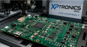
Overview of PCB Assembly at Xptronics
PCB assembly is the process of mounting electronic components onto a bare board to form a functional circuit. At Xptronics, we specialize in both Surface Mount Technology (SMT) and Through-Hole Technology (THT), as well as mixed-technology assemblies.
Our in-house capabilities allow us to serve a broad range of industries—from consumer electronics and telecommunications to industrial controls and automotive systems. Each project begins with a collaborative approach between our engineers, designers, and clients to ensure the best outcome for both performance and manufacturability.
Step 1: Design for Manufacturability (DFM) Review
Every successful assembly begins with a comprehensive DFM review. Before we begin the actual build, our engineers analyze the client’s design files—including Gerber data, Bill of Materials (BOM), and pick-and-place files—to identify any potential manufacturing issues.
Common checkpoints include:
- Component footprint accuracy
- Spacing for soldering and reflow
- Thermal profiling considerations
- Component availability and substitutions
By catching these issues early, we minimize delays, reduce rework, and improve yield.
Step 2: Material Procurement and Inventory Control
Our sourcing team works with a trusted network of authorized distributors to procure high-quality components. We prioritize:
- Authenticity (no grey-market parts)
- RoHS and REACH compliance
- Lot traceability
All incoming components are inspected visually and electronically before they are logged into our inventory system, which maintains FIFO (First In, First Out) practices and real-time traceability for every component batch used in a build.
Step 3: Solder Paste Application
For SMT boards, the first physical step is the solder paste application using an automated stencil printer. This process applies a precise amount of paste to each pad on the PCB to hold and electrically connect the components.
We use automated 2D and 3D paste inspection systems to verify correct volume, alignment, and thickness of solder paste. These checks are critical, as poor paste deposition is a leading cause of solder defects.
Step 4: Pick-and-Place Assembly
Once the paste is applied, the board moves to our automated pick-and-place machines, which place components—ranging from tiny 01005 resistors to large BGA packages—at high speed and with exceptional accuracy.
Key features of our placement systems include:
- Vision-assisted alignment
- Component presence verification
- Auto-correction for board skew
Our operators monitor machine performance in real time to ensure no misplaced or missing components escape attention.
Step 5: Reflow Soldering
The populated board is then passed through a multi-zone reflow oven, where the solder paste is melted and solidified, creating strong mechanical and electrical bonds.
Our ovens are programmable for:
- Lead-free (RoHS compliant) and leaded solder profiles
- Precise thermal ramp rates
- Peak temperature control to prevent component damage
Each product type has a custom thermal profile validated through thermocouple profiling.
Step 6: Through-Hole Component Insertion and Wave Soldering
For mixed-technology assemblies, through-hole components are inserted either manually or using semi-automatic insertion machines. The board then goes through wave soldering, where the underside of the board contacts a wave of molten solder to complete the joints.
Manual soldering is performed by our IPC-certified technicians for components that cannot be wave-soldered due to thermal sensitivity or odd shapes.
Step 7: Automated Optical Inspection (AOI)
After soldering, every board is inspected using Automated Optical Inspection (AOI) systems. AOI uses high-resolution cameras and algorithms to detect:
- Solder bridge and cold joints
- Incorrect or missing components
- Misalignments or tombstoning
- Polarity and orientation errors
AOI ensures defects are caught early, reducing the need for costly downstream rework.
Step 8: X-Ray Inspection (for BGA and Hidden Joints)
For assemblies with Ball Grid Array (BGA) or other hidden-lead components, we utilize X-ray inspection to examine the quality of solder joints beneath the package.
Our advanced X-ray machines allow for:
- 2D and angled imaging
- Void and bridging detection
- Quantitative analysis of joint integrity
X-ray inspection provides peace of mind that invisible solder connections are just as reliable as visible ones.
Step 9: Functional and In-Circuit Testing (FCT & ICT)
Where applicable, we offer both In-Circuit Testing (ICT) and Functional Circuit Testing (FCT). These are custom test stations built to validate:
- Electrical connectivity
- Proper voltage/current levels
- Functional behavior under load
- Firmware loading and communication checks
Testing is performed on a 100% basis for mission-critical assemblies or per batch for high-volume production.
Step 10: Final Inspection and Quality Control
Before shipping, every assembly undergoes a final visual inspection by our trained QA team. We follow IPC-A-610 standards (Acceptability of Electronic Assemblies), with Class 2 or Class 3 guidelines based on customer requirements.
Our inspectors verify:
- Cleanliness and conformal coating (if applicable)
- Labeling and serialization
- Connector integrity
- Cosmetic appearance
Once approved, the boards are packed in ESD-safe packaging and shipped with full documentation, including inspection reports and certificates of conformance.
Why Choose Xptronics for PCB Assembly?
At Xptronics, we go beyond just putting components on a board—we deliver complete manufacturing confidence. Our team combines technical expertise, modern equipment, and robust quality control to ensure every product performs reliably in the field.
Key advantages of working with Xptronics include:
- ISO-compliant processes
- IPC-certified operators and inspectors
- Traceability and transparency
- Rapid prototyping to full production
- North American-based customer service and logistics
Whether you need a few boards for a prototype or thousands for a production run, we scale with you—without compromising on quality.
Conclusion
The success of any electronic device depends on the integrity of its assembly. At Xptronics Inc., our PCB assembly and inspection processes are built around accuracy, reliability, and accountability. By investing in modern automation and skilled craftsmanship, we help our clients bring their designs to life with confidence.
Let us be your trusted partner in electronics manufacturing. Contact us today to learn more about how Xptronics can support your next project.