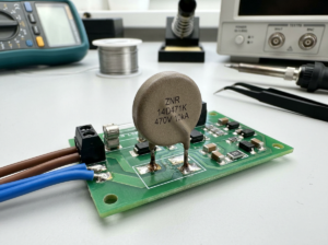
Designing electronics for hazardous environments goes far beyond standard PCB engineering. In industries such as oil and gas, mining, chemical processing, pharmaceuticals, and grain handling, equipment must be engineered to eliminate the risk of ignition. This is where intrinsically safe (IS) PCB I/O design becomes critical.
Intrinsically safe design ensures that electronic circuits are built in a way that limits electrical and thermal energy to levels incapable of igniting flammable gases, vapors, or dust. Instead of relying on explosion-proof enclosures, IS devices operate safely by design—making them lighter, more efficient, and easier to maintain.
Core Principles of Intrinsically Safe PCB I/O Design
1. Energy Limitation
The heart of an IS design is controlling energy. Components and I/O paths must restrict voltage, current, capacitance, and inductance to safe limits. Engineers use:
- Current-limiting resistors
- Zener diodes and avalanche protection
- Fuseable links
- Galvanic isolators
Every trace, connector, and interface must stay within safe energy budgets defined by IECEx, ATEX, and UL standards.
2. Galvanic Isolation
Isolation prevents dangerous faults from transferring from the safe side to the hazardous side. Typical methods include:
- Transformer-based isolation
- Optocouplers
- Digital isolators
Proper isolation protects both the user and the connected sensors or actuators in the hazardous area.
3. Fault Tolerance & Redundancy
IS circuits require single-fault safety, meaning even if one component fails, the device must remain safe. Engineers design for:
- Redundant current-limiting components
- Fail-safe transient protection
- Protected ground return paths
- Derating of components for heat and stress
4. Thermal Management
Even small amounts of power can create heat capable of igniting a hazardous atmosphere. Careful attention must be paid to:
- Component placement
- Trace width to minimize I²R heating
- Limiting allowed power dissipation
- Thermal runaway prevention
- Enclosure temperature classification (T-ratings)
5. Control of Stored Energy
Capacitors and inductors can store energy that could discharge during a fault. This requires:
- Strict selection of component values
- Energy calculation per safety standards
- Fast-acting suppression circuits
Every µJ must be accounted for.
I/O Interface Considerations
When designing I/O (inputs and outputs) for intrinsically safe PCBs, each interface needs careful engineering:
Sensor Inputs
Low-level signals must be filtered and protected while maintaining accuracy. Typical techniques include:
- RC/LC filtering
- Transient voltage suppressors
- Barrier networks to limit fault energy
Outputs to Field Devices
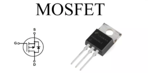
Driving solenoids, LEDs, and actuators requires special attention:
- Controlled current drivers
- Series resistors to restrict fault currents
- Certified intrinsically safe output stages
Communication Interfaces
For RS-485, CANbus, or 4–20 mA loops in hazardous zones:
- Intrinsically safe isolators
- Ex-approved interface modules
- Shielding and grounding strategies to avoid unintended coupling
Why Intrinsically Safe Design Matters
Modern industrial facilities are pushing for greater automation, smarter sensing, and real-time monitoring. Intrinsically safe PCB I/O design enables these advancements without compromising safety. Benefits include:
- Lower certification and installation costs than explosion-proof designs
- Higher equipment reliability
- Reduced maintenance downtime
- Increased worker safety
PCBA at XPtronics Inc
At XPtronics Inc, we specialize in assembling electronics that meet stringent industrial safety standards. Our engineering and PCBA expertise ensures your devices are safe, compliant, and production-ready.
If your technology must operate in hazardous environments, we can help you build it with confidence.