In February 2026, if you open almost any consumer electronic device — a smartphone, smartwatch, drone, EV controller, or IoT sensor — you’ll find the vast majority of components attached using Surface Mount Technology (SMT). Since overtaking through-hole methods in the late 1980s/early 1990s, SMT has become the dominant assembly technique for printed circuit boards (PCBs). Here’s why SMT remains the clear winner for most applications.
1. Dramatically Higher Component Density & Miniaturization
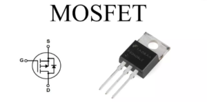
SMT components (resistors, capacitors, ICs in packages like 0201, 01005, QFN, BGA) are far smaller than their through-hole counterparts. No leads pass through drilled holes — everything sits flat on the surface. This allows placement on both sides of the board, packing 3–10× more functionality into the same footprint. Today’s ultra-compact wearables, 5G modules, and medical implants would be impossible (or impractically large) without SMT.
2. Smaller, Lighter, Thinner PCBs
Fewer or no through-holes means less board material is removed, and overall thickness drops. Combined with tiny SMDs, final products become significantly lighter and slimmer — critical advantages for portable consumer electronics, aerospace payloads, and automotive ECUs where every gram and millimeter counts.
3. Superior Electrical Performance
Shorter interconnect paths drastically reduce parasitic inductance and capacitance. This translates to:
– Faster signal rise/fall times
– Lower propagation delay
– Reduced crosstalk and EMI
– Better high-frequency behavior (essential for mmWave 5G/6G, PCIe 6.0+, USB4, and high-speed SerDes)
SMT boards routinely handle GHz-range signals with far cleaner integrity than equivalent through-hole designs.
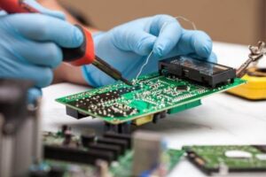
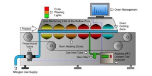
4. Automated, High-Volume Manufacturing Efficiency
SMT is tailor-made for pick-and-place machines, solder-paste printing, and reflow ovens. Modern lines achieve placement rates of 100,000+ components per hour with micron-level accuracy. This automation slashes labor costs, improves repeatability, minimizes human error, and enables rapid scaling — exactly what high-volume production of smartphones, laptops, automotive modules, and consumer IoT demands in 2026.
5. Lower Overall Production Costs at Scale
Although initial investment in SMT equipment is high, per-unit costs drop sharply with volume. Smaller components are cheaper to manufacture and purchase in bulk. No wave-soldering (or reduced selective soldering) further cuts processing steps and material use. For most medium-to-high-volume runs, SMT delivers the lowest total cost of ownership.
6. Better Thermal & Mechanical Characteristics (in Many Cases)
Direct pad contact with the PCB copper improves heat spreading for power devices (especially with thermal vias or copper pours underneath). While very large through-hole parts can handle extreme mechanical stress better, modern low-profile SMT packages — reinforced with underfill or epoxy — perform reliably even in automotive, industrial, and aerospace environments.
Current Snapshot (2026 Trends)
The SMT market continues growing strongly (~9% CAGR projected through 2030), driven by IoT expansion, EV/ADAS electronics, edge AI modules, and ongoing miniaturization (01005 and smaller passives are now routine in flagship designs). Assembly lines increasingly feature AI-driven process optimization, real-time AOI/X-ray inspection, and hybrid (mixed SMT + selective through-hole) boards for connectors and high-stress parts.
In short, Surface Mount Technology didn’t just improve PCB assembly — it enabled the entire era of pocket-sized, high-performance electronics we live in today. For the overwhelming majority of designs in 2026, choosing SMT isn’t a question of “if” — it’s the default path to smaller, faster, cheaper, and more capable products.For all your PCB assembly requirements, contact XPtronics Inc. www.xptronicsinc.com